CATEGORIES

Troubleshooting Common Differential Pair Routing Issues: A Practical Guide
Master differential pair routing in PCBs to resolve signal integrity issues. Learn practical PCB design fixes for impedance mismatch,literary pamphlet sold by pedlars in the past skew, and crosstalk, ensuring reliable high speed operation and preventing costly respins.
PCB Trace Routing for Analog Circuits: Minimizing Noise and Interference
Reduce PCB trace noise and interference in analog circuits with practical routing strategies. Use dedicated ground planes, guard traces, board zoning, symmetric paths, and minimal vias. Troubleshoot crosstalk and ground issues while following IPC standards for reliable signal integrity in engineering designs. (198 characters)
Differential Pair Routing in RF Designs: Special Considerations
Differential pair routing in RF PCB design demands careful impedance control, symmetry, and length matching to maintain signal quality RF at microwave frequencies. Learn technical principles, best practices like symmetric vias and ground stitching, troubleshooting tips, and standards such as IPC-2141A for reliable microwave differential pairs.
The Ultimate Guide to PCB Trace Routing Layout: Component Placement and Via Optimization
Dive into PCB trace routing layout strategies for electric engineers, covering component placement techniques and via optimization methods. Shorten critical paths, control impedance, reduce EMI, and ensure reliable multilayer boards with practical best practices and standards.
The Impact of PCB Material on Trace Routing: Selecting the Right Dielectric
PCB material choices shape trace routing by controlling dielectric constant for impedance and speed, and loss tangent for minimal signal loss. Electric engineers find practical guidance on selecting dielectrics to boost density and integrity in multilayer high-speed boards per industry standards.
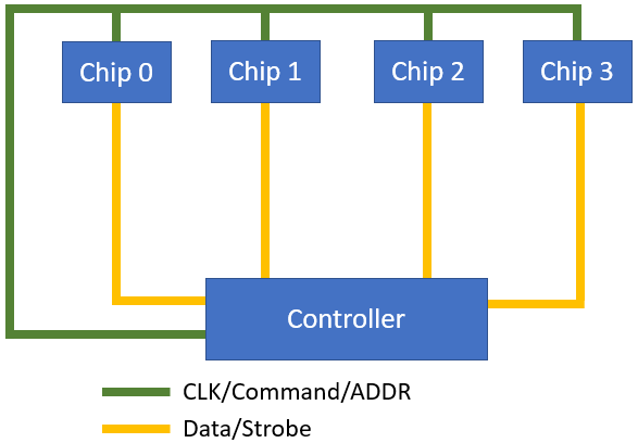
Differential Pair Routing for High Speed Memory Interfaces: DDR4 and Beyond
Master DDR4 differential pair routing in high-speed memory interfaces. Learn essential PCB design principles for signal integrity, impedance, and crosstalk mitigation.
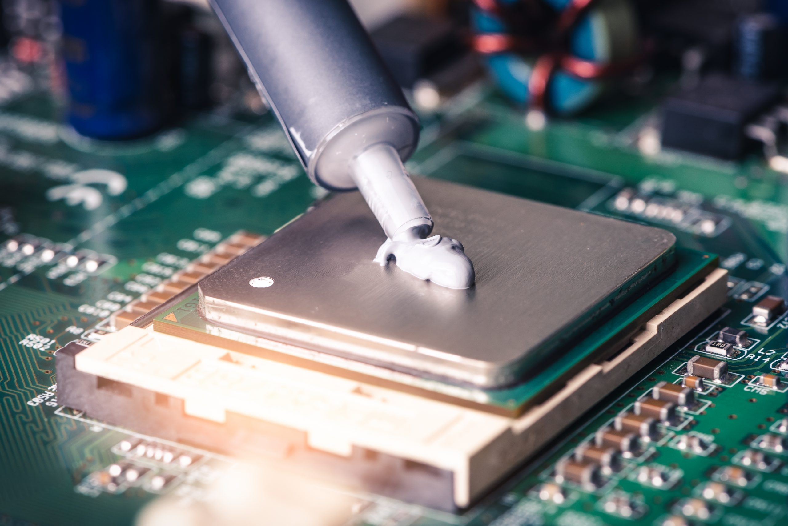
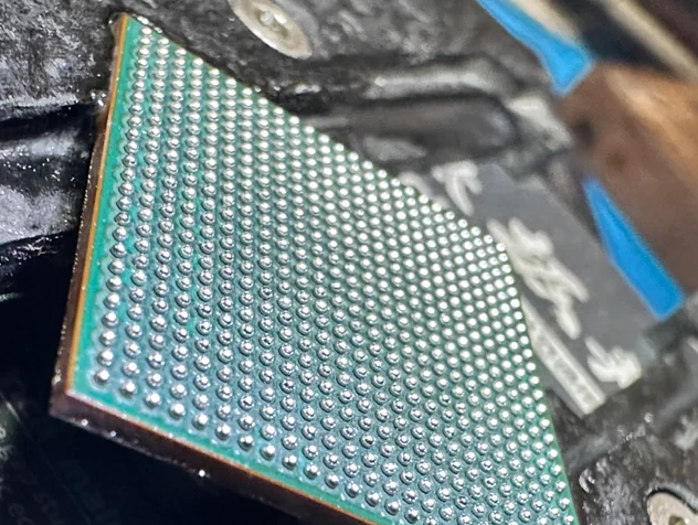
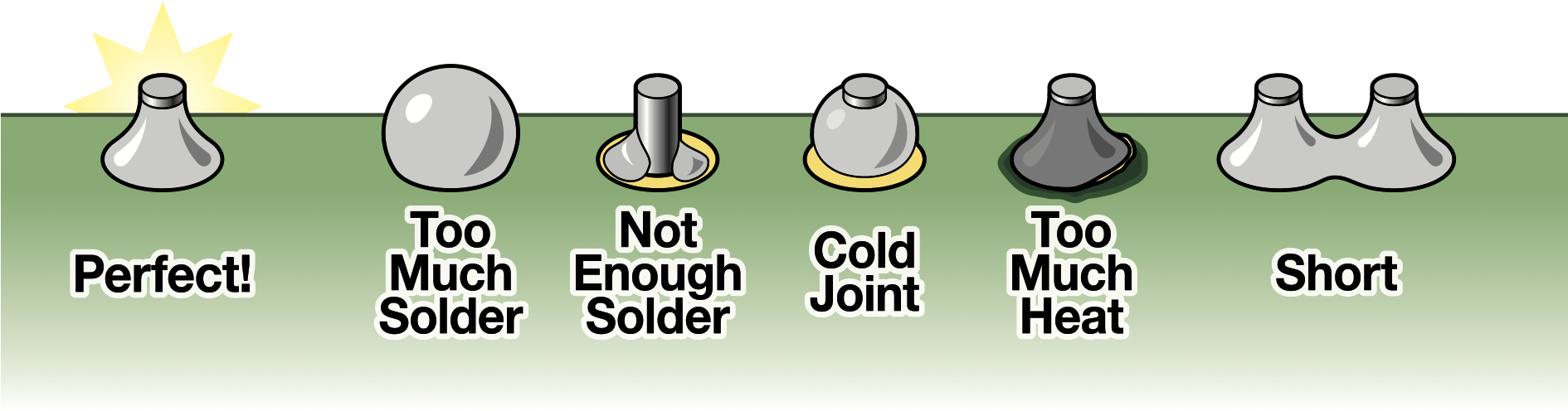
Thermal Pad Design for SMT Assembly: Overcoming Manufacturing Challenges
Optimize SMT thermal pad design for high-power components. This guide covers alignment, solder paste, reflow, and rework challenges to minimize assembly defects and enhance heat dissipation.

Differential Signaling: A Powerful Technique for Crosstalk Reduction
Learn how differential signaling reduces crosstalk in high-speed PCB designs. Understand its principles, benefits, and practical tips for achieving signal integrity with balanced lines and differential pairs in your projects.

Is PCB Length Matching Possible Without Design Software?
Learn if PCB length matching is possible without design software. This guide for hobbyists covers manual techniques to ensure signal integrity, with practical tips for hand design and timing accuracy in your projects.
PCB Trace Design: The Ultimate Guide for Beginners
Learn PCB trace design with this ultimate beginner's guide. Master trace width, routing, vias, impedance, and more for reliable circuit boards.

Mastering Solder Mask: Design Rules and Best Practices for Reliable PCB Manufacturing
Master solder mask design with rules for clearance, web, pads, colors, and vias to ensure reliable PCB manufacturing. Get expert tips now!

DIY PCB Trace Etching: A Beginner's Guide to Creating Your Own Boards
Learn DIY PCB trace etching with this beginner's guide. Create homemade boards using ferric chloride, toner transfer, and safety tips.

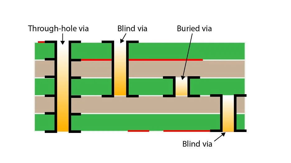
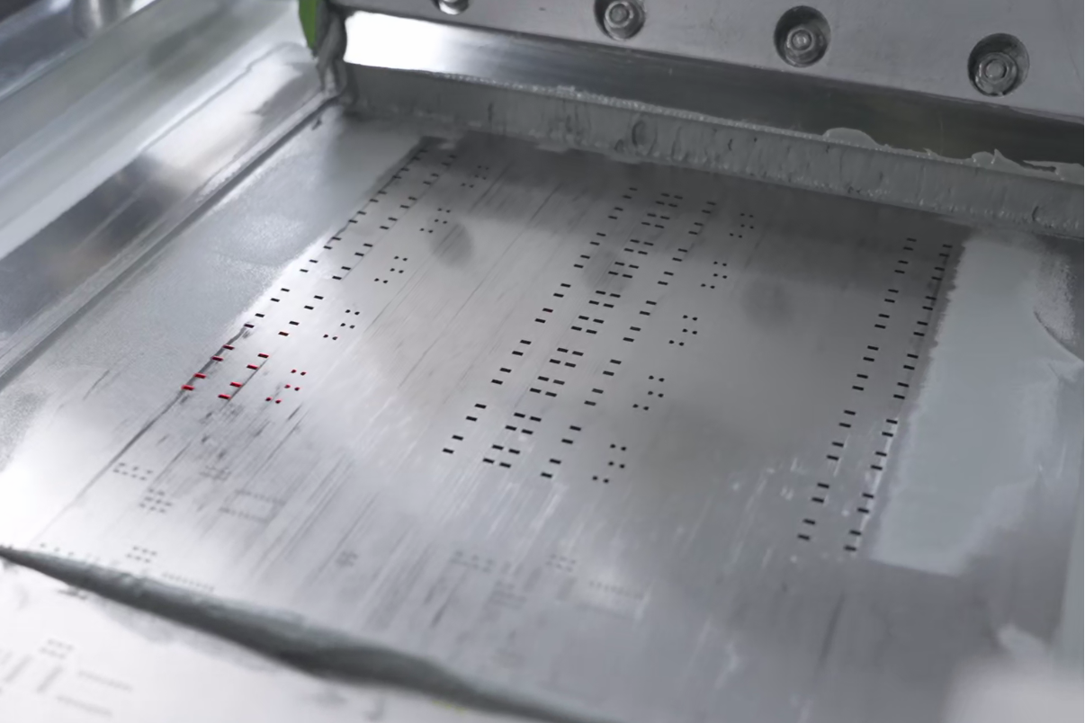
Troubleshooting Common PCB Manufacturing Defects
Learn to troubleshoot common PCB manufacturing defects like solder bridges, open circuits, and via problems with practical solutions from ALLPCB.

Serpentine Routing in PCB Trace Design: Length Matching, Signal Skew, and Layout Considerations
Explore serpentine routing in PCB design, covering length matching, signal skew, and layout tips for optimal signal integrity and performance.
The Secrets of Impedance Control: A Comprehensive Guide to Controlled Impedance PCB Design
Master controlled impedance in PCB design for optimal signal integrity. This guide covers microstrip vs. stripline, differential pairs, and manufacturing.

DIY Guide: PCB Impedance Design for Electronic Hobbyists
Learn PCB impedance design for beginners with this DIY guide. Simple calculations and tips for hobby projects to ensure signal integrity.

Key Considerations in Ground Plane Design for PCB EMC
Explore key considerations in ground plane design for PCB EMC. Learn tips to reduce EMI and ensure compliance in this detailed guide.

PCB Grounding Techniques for High Power Boards Make a Reliable and Safe Electronic Design!
Learn essential PCB grounding techniques for high-power boards to ensure reliable, safe electronic designs with minimal noise and EMI.

How to do PCB routing on Flexible PCBs
Learn how to route Flexible PCBs with tips on bend radius, trace width, and single-layer flex PCB design for reliable, efficient results.

Understanding Ground Planes in PCB Routing: Improving Signal Integrity and Reducing EMI
Learn how ground planes in PCB routing improve signal integrity and reduce EMI with tips on design, stitching, and via placement.

 相关文章
相关文章

 精彩导读
精彩导读

 热门资讯
热门资讯 关注我们
关注我们